Features of Infrared Laser Scanning Confocal Microscopes
May 7th 2023
Features and Benefits of the Infrared Laser Scanning Confocal Microscope
Semiconductor wafers, bonded wafer "sandwiches," and other microelectronic devices often require the ability to perform examinations to maintain "Quality in Process." This means that wafers, at any step in the manufacturing process, might need to be inspected, or measured, or both in a non-destructive manner, to assure that geometries are properly sized, and to confirm any overlay registration alignment is within specification. Also, a method to investigate for contamination on any layer will be helpful to confirm a level of technical cleanliness, or to determine porosity in the adhesion of a bonded device.
Further, there is also the need to perform a forensic evaluation due to a device failure. This can be from a current lot of tested devices; one that functionally failed under an electrical load; or one that was deployed to a customer, which prematurely failed and was returned to the manufacturer for a "Root Cause" analysis.
The video below shows an operator select preset focal planes on both sides of a bonded wafer sandwich focusing right through the substrate. The contrast and image quality of the Infrared Laser Scanning Confocal Microscope system is absolutely remarkable for a NIR-based imaging system.
10x Objective Over and Under Registration Fiducials IR-LSCM
20x Objective Over and Under Registration Fiducials IR-LSCM
The Infrared Laser Scanning Confocal Microscope allows for the imaging through multiple layers of various substrates including silicon, glass, sapphire, Silicon Carbide, and other exotic materials. Device types often inspected here include full wafers, wafer bonding, IC chips, MEMS devices, photovoltaic and Solar panels, and more. Near-IR laser and IR optics coupled with confocal scanning technology are ideal for non-destructive subsurface interior investigation of these devices. Alignment fiducials are now clearly seen and easily measured for the offset to confirm registration.
Infrared Laser Scanning Confocal Microscope Images
The images captured below show the infrared laser scanning confocal microscope in action.
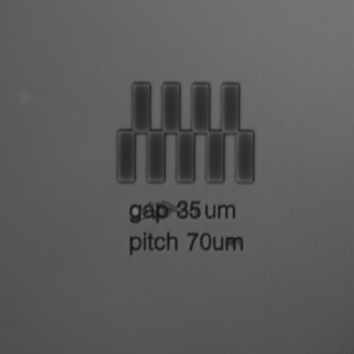
Front Side Fiducial - Infrared Confocal 20x Objective Lens.
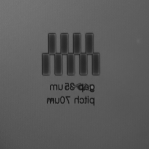
Back Side Fiducial - Infrared Confocal 20x Objective Lens (Inverted Image).
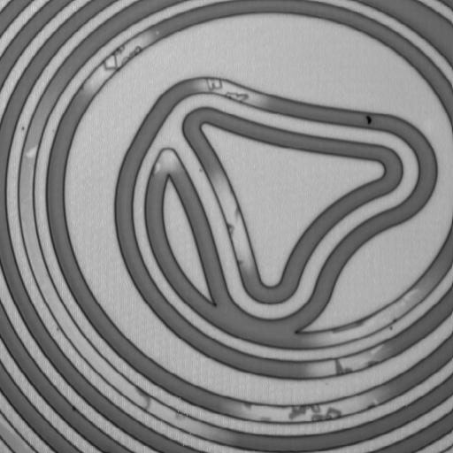
Front Side MEMS Spring Delamination - Infrared Confocal 20x Objective Lens.
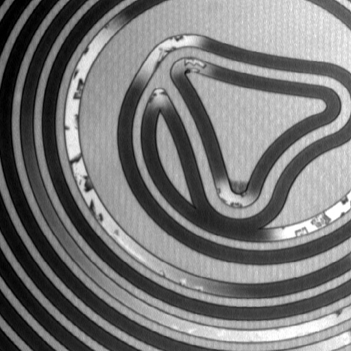
Back Side MEMS Spring Delamination - Infrared Confocal 20x Objective Lens.
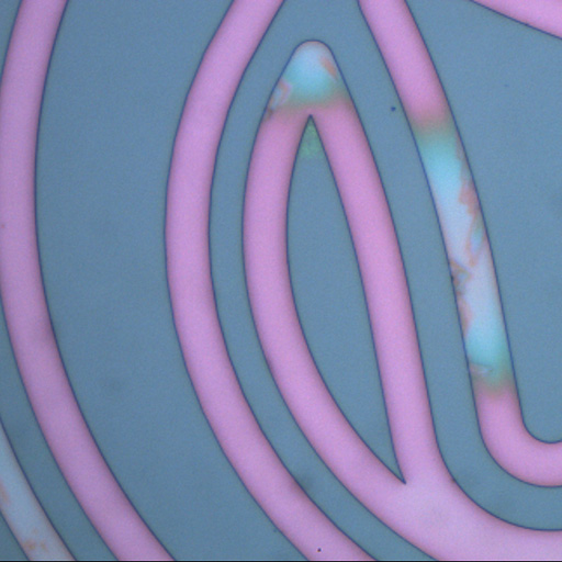
Front Side MEMS Sprig Delamination - Visual White-Light Imaging 20x Objective Lens.
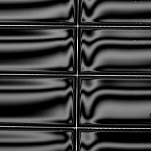
IR Mesa Positive Resist - Infrared Confocal 5x Objective Lens.
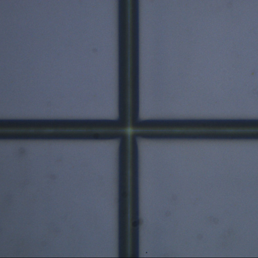
IR Mesa Positive Resist - Visual White-Light Imaging 10x Objective Lens.
The IR-LSCM features a full automation package consisting of a motorized XY stage, objective lens turret, illumination, motorized focus, and laser attenuation. Powerful yet intuitive software is included, designed to increase the effectiveness and efficiency of the inspection and review processes. Optional automation and recipe software is available, allowing the system to conduct completely automated inspection routines on individual devices or complete wafers and/or IC strip and tray packages. Contact Microscope World today for an Application Study to show how the IR-LCSM will enable the inspection and registration measurement of your critical devices!


